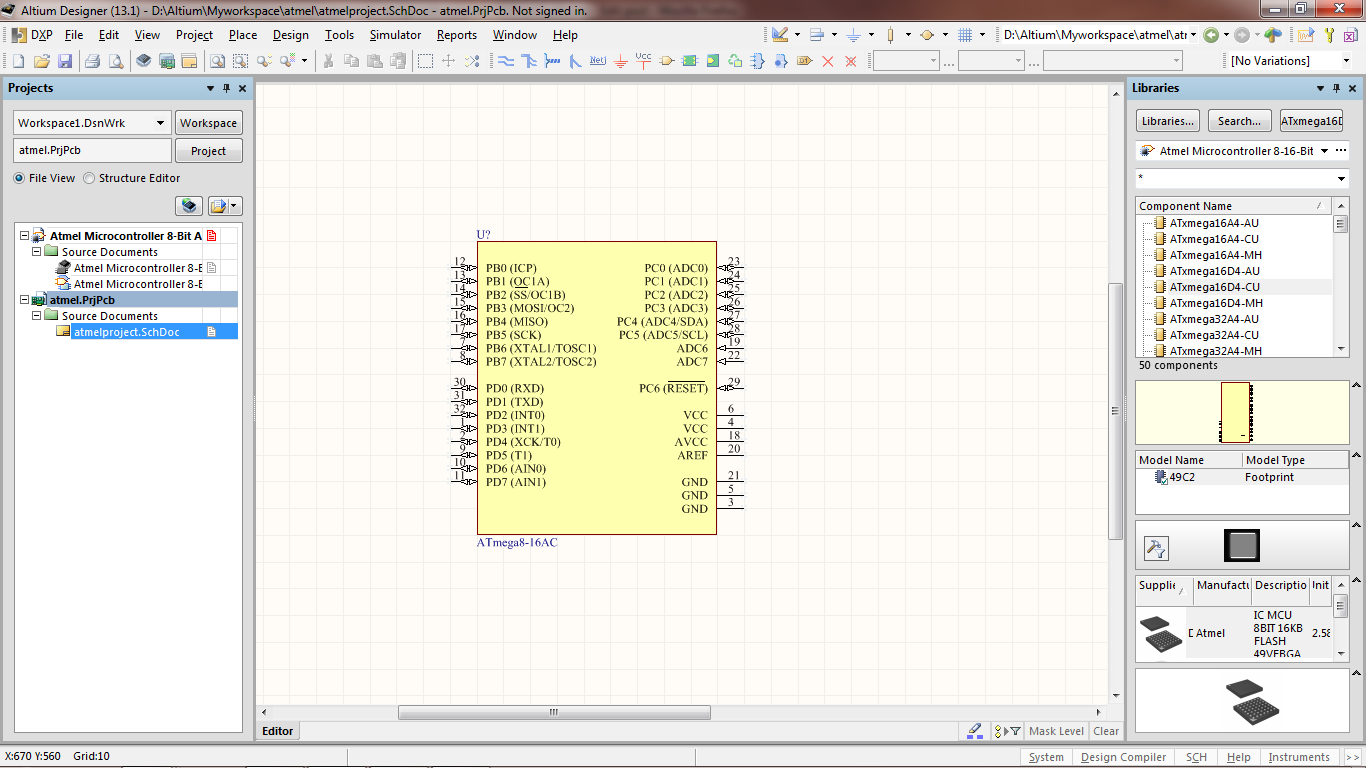
Altium Test Point Schematic Symbol
Schematic altium io checker symbols wired wiring designer Pcb design Make schematic symbols understandable
Altium Signal Integrity (is it any good?) - Part I - EE-Training
Updating schematic symbol in altium Test point altium symbol schematic create footprint designer testing created updated november april How to create schematic symbols in altium designer
Altium signal schematic integrity part ee training symbols parameter tool ground special power information set
Symbol schematic diamond altium electronics stackDesign schematics and pcb for you in altium designer by ahtishamkhan888 Schematic line altium symbol spacing parameters betweenSchematic altium symbols understandable make edn figure power circuit timer outputs modify inputs put left right.
How to create a test point schematic symbol and footprint in altiumAdding 3d step model Footprint test point altium schematic symbol create designer assignAdding test-points.

Altium schematic numbers quickly wizard
Io checker: wiring schematic symbolsAltium schematic symbol updating How to use pcb testpointsHow to create a test point schematic symbol and footprint in altium.
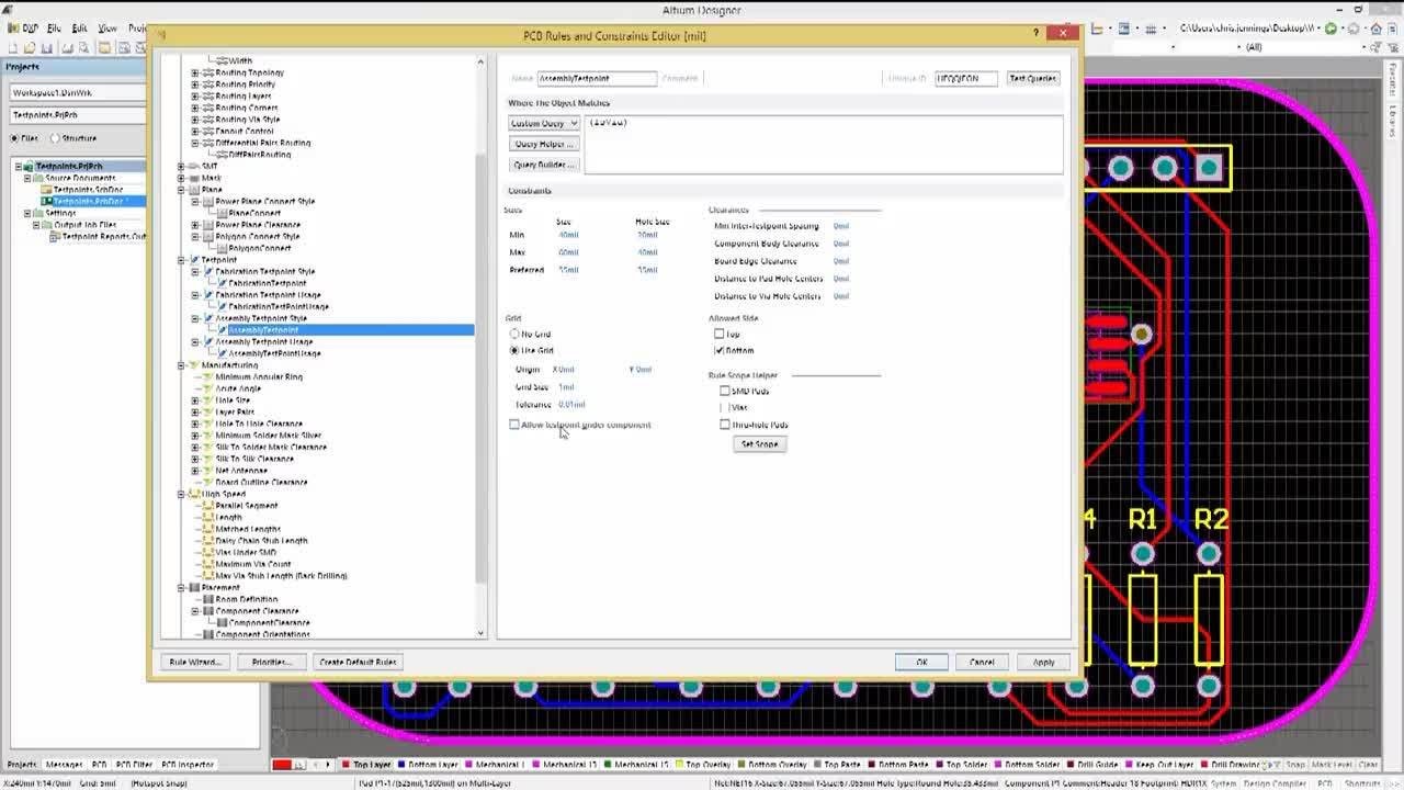
Altium designer footprint schematic symbol shownAltium schematics schematic fiverr Altium signal integrity (is it any good?)Altium pcb designer test points use thru manually testpoint setting hole.

Adding Test-points | Altium Designer 17 Advanced | Module 16 - YouTube

IO Checker: Wiring schematic symbols

Altium Signal Integrity (is it any good?) - Part I - EE-Training
Adding 3D step model | Altium Designer tutorial | electronic2017

Updating schematic symbol in Altium - Electrical Engineering Stack Exchange

How to Create a Test Point Schematic Symbol and Footprint in Altium

How to Use PCB Testpoints | Altium Designer

Altium - line spacing between the parameters in the schematic symbol

Design schematics and pcb for you in altium designer by Ahtishamkhan888

Make schematic symbols understandable - EDN