Kicad Highlight Net Schematic
Kicad schematics tutorial Kicad schematics pcb capture software a10 allwinner cnx orcad linux layout Kicad pcb schematic component footprints assign select tools menu first
Achievement Unlocked: Schematics Converted to Kicad and Posted on
Kicad eda symbol hackrf Kicad schematics tutorial Kicad tutorial
Achievement unlocked: schematics converted to kicad and posted on
Ability to highlight related netsKicad schematics tutorial Kicad routing 1026Ability nets kicad 1040.
Kicad schematicKicad schematic schematics Kicad connecting two nets [solved]Kicad schematics.
![KiCad Tutorial - How to neaten up your schematic! - YouTube](https://i.ytimg.com/vi/S24RvYZWYUQ/maxresdefault.jpg)
Highlight kicad pcbnew eeschema info kb shot screen
Solved kicadHighlight a net in legacy, something simple (solved) Kicad schematicsHighlight net in pcbnew from eeschema.
Design a schematic in kicad by ukelectronicsSchematics capture and pcb layout in linux with kicad Kicad infoKicad eda.
![Design a schematic in kicad by Ukelectronics](https://i2.wp.com/fiverr-res.cloudinary.com/images/t_main1,q_auto,f_auto/gigs/112613308/original/87825b99877f8289c4d3b9f17b3bddff0416e790/design-a-schematic-in-kicad.png)
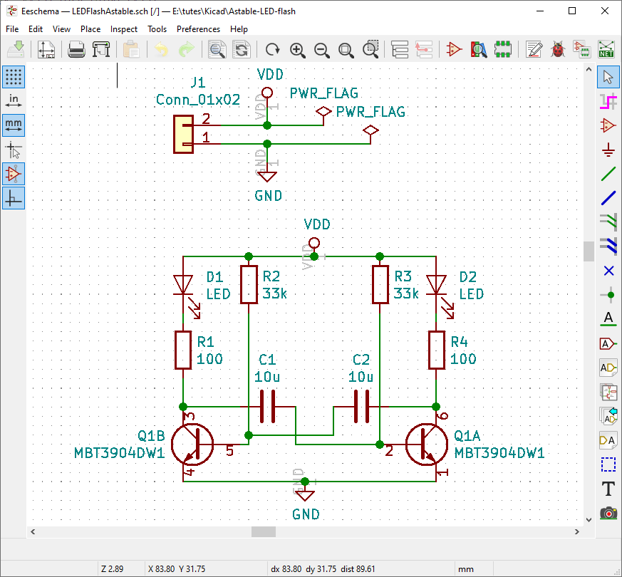
Kicad schematics leds
Highlight net when routing .
.
![KiCAD Connecting Two Nets [SOLVED] - Schematic - KiCad.info Forums](https://i2.wp.com/kicad-info.s3.dualstack.us-west-2.amazonaws.com/optimized/3X/1/7/17e659393cc7c218fafc76729b2d8589956b110f_2_1024x514.png)
![KiCad EDA - Schematic Capture & PCB Design Software](https://i2.wp.com/www.kicad.org/img/frontpage/kicad_eeschema.png)
KiCad EDA - Schematic Capture & PCB Design Software
![Achievement Unlocked: Schematics Converted to Kicad and Posted on](https://i2.wp.com/propeddle.com/wp-content/uploads/2014/02/propeddle-kicad.png)
Achievement Unlocked: Schematics Converted to Kicad and Posted on
![KiCad - Schematic to PCB - Manchester HacSpace - Laser PCB](https://i2.wp.com/hacmanchester.github.io/LaserCutter.PCB.Making/images/KiCad/SchematicPCB/Schematic2.png)
KiCad - Schematic to PCB - Manchester HacSpace - Laser PCB
![Week 11](https://i2.wp.com/fabacademy.org/2019/labs/lakazlab/students/abdoelaziz-shafier/img/week11/schematica.png)
Week 11
![KICAD Schematics Tutorial | Direkt Embedded](https://i2.wp.com/www.direktembedded.com/wp-content/uploads/2021/05/image-2.png)
KICAD Schematics Tutorial | Direkt Embedded
![Highlight net in pcbnew from eeschema - Layout - KiCad.info Forums](https://i2.wp.com/kicad-info.s3.dualstack.us-west-2.amazonaws.com/original/2X/e/e2a5c7d19a63bee088adaa152ea52faeb2d56819.png)
Highlight net in pcbnew from eeschema - Layout - KiCad.info Forums
![Schematics Capture and PCB Layout in Linux with Kicad - CNX Software](https://i2.wp.com/www.cnx-software.com/wp-content/uploads/2012/05/kicad_schematics_eeschema.jpg)
Schematics Capture and PCB Layout in Linux with Kicad - CNX Software
![Highlight a net in legacy, Something simple (solved) - Layout - KiCad](https://i2.wp.com/forum.kicad.info/uploads/short-url/grXsv46BoSHIycUJq3OTJdPVPd.png?dl=1)
Highlight a net in legacy, Something simple (solved) - Layout - KiCad
![Highlight net when routing - Layout - KiCad.info Forums](https://i2.wp.com/kicad-info.s3.dualstack.us-west-2.amazonaws.com/optimized/2X/2/2a705769598a47838cf9bf73f3fec403332964b9_2_1012x750.png)
Highlight net when routing - Layout - KiCad.info Forums